- 您现在的位置:买卖IC网 > Sheet目录2006 > LTC2621IDD-1#PBF (Linear Technology)IC DAC 12BIT R-R 10-DFN
LTC2601/LTC2611/LTC2621
5
2601fb
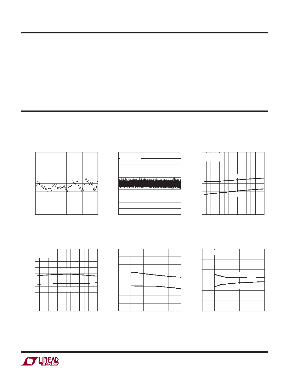
TYPICAL PERFORMANCE CHARACTERISTICS
Integral Nonlinearity (INL)
Differential Nonlinearity (DNL)
INL vs Temperature
DNL vs Temperature
INL vs VREF
DNL vs VREF
TIMING CHARACTERISTICS
Note 1: Stresses beyond those listed under Absolute Maximum Ratings
may cause permanent damage to the device. Exposure to any Absolute
Maximum Rating condition for extended periods may affect device
reliability and lifetime.
Note 2: Linearity and monotonicity are dened from code KL to code
2N – 1, where N is the resolution and KL is given by KL = 0.016(2N/VREF),
rounded to the nearest whole code. For VREF = 4.096V and N = 16, KL =
256 and linearity is dened from code 256 to code 65,535.
Note 3: Digital inputs at 0V or VCC.
Note 4: Guaranteed by design and not production tested.
Note 5: Inferred from measurement at code KL = 0.016(2N/VREF) and at
full scale.
Note 6: VCC = 5V, VREF = 4.096V. DAC is stepped 1/4 scale to 3/4 scale and
3/4 scale to 1/4 scale. Load is 2k in parallel with 200pF to GND.
Note 7: VCC = 5V, VREF = 4.096V. DAC is stepped ±1LSB between half scale
and half scale – 1. Load is 2k in parallel with 200pF to GND.
Note 8: These specications apply to LTC2601/LTC2601-1,
LTC2611/LTC2611-1, LTC2621/LTC2621-1
LTC2601
CODE
0
16384
32768
49152
65535
INL
(LSB)
2601 G01
32
24
16
8
0
–8
–16
–24
–32
VCC = 5V
VREF = 4.096V
CODE
0
16384
32768
49152
65535
DNL
(LSB)
2600 G02
1.0
0.8
0.6
0.4
0.2
0
–0.2
–0.4
–0.6
–0.8
–1.0
VCC = 5V
VREF = 4.096V
TEMPERATURE (°C)
–50
–30
–10
10
30
50
70
90
INL
(LSB)
2601 G03
32
24
16
8
0
–8
–16
–24
–32
VCC = 5V
VREF = 4.096V
INL (POS)
INL (NEG)
TEMPERATURE (°C)
–50
–30
–10
10
30
50
70
90
DNL
(LSB)
2601 G04
1.0
0.8
0.6
0.4
0.2
0
–0.2
–0.4
–0.6
–0.8
–1.0
VCC = 5V
VREF = 4.096V
DNL (POS)
DNL (NEG)
VREF (V)
0
1
2
3
4
5
INL
(LSB)
2601 G05
32
24
16
8
0
–8
–16
–24
–32
VCC = 5.5V
INL (POS)
INL (NEG)
VREF (V)
0
1
2
3
4
5
DNL
(LSB)
2601 G06
1.5
1.0
0.5
0
–0.5
–1.0
–1.5
VCC = 5.5V
DNL (POS)
DNL (NEG)
发布紧急采购,3分钟左右您将得到回复。
相关PDF资料
LTC2630HSC6-LZ12#TRPBF
IC DAC 12BIT R-R SC70-6
LTC2642IDD-16#PBF
IC DAC 16BIT VOUT 10-DFN
LTC2704IGW-16#PBF
IC DAC 16BIT QUAD VOUT 44-SSOP
LTC2751AIUHF-16#PBF
IC DAC 16BIT CUR OUT 38-QFN
LTC2752ACLX#PBF
IC DAC 16BIT DUAL CUR OUT 48LQFP
LTC2753AIUK-16#TRPBF
IC DAC 16BIT DUAL 48-QFN
LTC2754AIUKG-16#PBF
IC DAC 16BIT QUAD IOUT 52-QFN
LTC2755AIUP-16#PBF
IC DAC 16BIT CUR OUT 64-QFN
相关代理商/技术参数
LTC2621IDD-1#TRPBF
功能描述:IC DAC 12BIT SGL R-R VOUT 10DFN RoHS:是 类别:集成电路 (IC) >> 数据采集 - 数模转换器 系列:- 产品培训模块:Data Converter Fundamentals
DAC Architectures 设计资源:Unipolar, Precision DC Digital-to-Analog Conversion using AD5450/1/2/3 8-14-Bit DACs (CN0052)
Precision, Bipolar, Configuration for AD5450/1/2/3 8-14bit Multiplying DACs (CN0053)
AC Signal Processing Using AD5450/1/2/3 Current Output DACs (CN0054)
Programmable Gain Element Using AD5450/1/2/3 Current Output DAC Family (CN0055)
Single Supply Low Noise LED Current Source Driver Using a Current Output DAC in the Reverse Mode (CN0139) 标准包装:10,000 系列:- 设置时间:- 位数:12 数据接口:DSP,MICROWIRE?,QSPI?,串行,SPI? 转换器数目:1 电压电源:单电源 功率耗散(最大):- 工作温度:-40°C ~ 125°C 安装类型:表面贴装 封装/外壳:SOT-23-8 薄型,TSOT-23-8 供应商设备封装:TSOT-23-8 包装:带卷 (TR) 输出数目和类型:1 电流,单极;1 电流,双极 采样率(每秒):2.7M
LTC-2621JD
功能描述:LED 显示器和配件 3 Digit, Red Low Current RoHS:否 制造商:Avago Technologies 显示器类型:7 Segment 数位数量:2 字符大小:7.8 mm x 14.22 mm 照明颜色:Red 波长:628 nm 共用管脚:Common Anode 工作电压:2.05 V 工作电流:20 mA 最大工作温度:+ 85 C 最小工作温度:- 35 C 封装:Tube
LTC-2621JD-01
制造商:Lite-On Semiconductor Corporation 功能描述:DISPLAY,CLOCK,3-DIG,ALINGAP RED,LOW-CUR,0.28",CAMPX - Rail/Tube
LTC-2621P
功能描述:LED 显示器和配件 3 Digit, Red RoHS:否 制造商:Avago Technologies 显示器类型:7 Segment 数位数量:2 字符大小:7.8 mm x 14.22 mm 照明颜色:Red 波长:628 nm 共用管脚:Common Anode 工作电压:2.05 V 工作电流:20 mA 最大工作温度:+ 85 C 最小工作温度:- 35 C 封装:Tube
LTC-2621WC
功能描述:LED 显示器和配件 3 Digit, Red Low Current RoHS:否 制造商:Avago Technologies 显示器类型:7 Segment 数位数量:2 字符大小:7.8 mm x 14.22 mm 照明颜色:Red 波长:628 nm 共用管脚:Common Anode 工作电压:2.05 V 工作电流:20 mA 最大工作温度:+ 85 C 最小工作温度:- 35 C 封装:Tube
LTC-2621Y
功能描述:LED 显示器和配件 3 Digit, Yellow RoHS:否 制造商:Avago Technologies 显示器类型:7 Segment 数位数量:2 字符大小:7.8 mm x 14.22 mm 照明颜色:Red 波长:628 nm 共用管脚:Common Anode 工作电压:2.05 V 工作电流:20 mA 最大工作温度:+ 85 C 最小工作温度:- 35 C 封装:Tube
LTC2622CMS8
功能描述:IC DAC 12BIT DUAL R-R VOUT 8MSOP RoHS:否 类别:集成电路 (IC) >> 数据采集 - 数模转换器 系列:- 产品培训模块:LTC263x 12-, 10-, and 8-Bit VOUT DAC Family 特色产品:LTC2636 - Octal 12-/10-/8-Bit SPI VOUT DACs with 10ppm/°C Reference 标准包装:91 系列:- 设置时间:4µs 位数:10 数据接口:MICROWIRE?,串行,SPI? 转换器数目:8 电压电源:单电源 功率耗散(最大):2.7mW 工作温度:-40°C ~ 85°C 安装类型:表面贴装 封装/外壳:14-WFDFN 裸露焊盘 供应商设备封装:14-DFN-EP(4x3) 包装:管件 输出数目和类型:8 电压,单极 采样率(每秒):*
LTC2622CMS8#PBF
功能描述:IC DAC 12BIT DUAL R-R VOUT 8MSOP RoHS:是 类别:集成电路 (IC) >> 数据采集 - 数模转换器 系列:- 产品培训模块:Lead (SnPb) Finish for COTS
Obsolescence Mitigation Program 标准包装:50 系列:- 设置时间:4µs 位数:12 数据接口:串行 转换器数目:2 电压电源:单电源 功率耗散(最大):- 工作温度:-40°C ~ 85°C 安装类型:表面贴装 封装/外壳:8-TSSOP,8-MSOP(0.118",3.00mm 宽) 供应商设备封装:8-uMAX 包装:管件 输出数目和类型:2 电压,单极 采样率(每秒):* 产品目录页面:1398 (CN2011-ZH PDF)